There has been much recent progress in the trapping and cooling of neutral atoms, opening up new areas of ultra-low energy and matter-wave physics [45,51,159]. Waveguides for such atoms are of great interest for atom optics, atom interferometery, and atom lithography. Multimode atom waveguides act as incoherent atom pipes that could trap atoms, transport them along complicated paths or between different environments, or deliver highly localized atom beams to a surface. Single-mode waveguides (or multimode guides populated only by atoms in the transverse ground-state) could be used for coherent atom optics and interferometry [151,2], as well as a tool for one-dimensional physics such as boson-fermion duality [190,152,44] and low-dimensional Bose-Einstein condensation effects [115].
The optical dipole-force has long been used to trap and manipulate atoms [45,51,159] as well as dielectric particles [9,113] (for a review see [10]). The available intensity of lasers has allowed a multitude of such atom traps in the far-detuned regime, giving very low decoherence and heating rates, and storage times on the order of seconds (for a review of dipole-force atom trapping, see [85]).
Evanescent light waves have been popular in many
atom mirrors, traps and guides (see the original
theoretical work [52,13]
and review [67])
since they can provide potentials with
high spatial gradients (decay lengths
![]() where
where ![]() is the optical wavelength),
and use rigid
dielectric structures (prisms, fibers)
to define the potential shape.
For example,
there has been a series of repulsive (blue-detuned)
evanescent-wave (EW) traps which rely on gravity to
provide the counteracting force [4,155]
and
recent
experiments have shown that hollow optical fibers can guide
atoms confined within the
hollow core using a repulsive evanescent field guided
by the fiber [170,102,103].
is the optical wavelength),
and use rigid
dielectric structures (prisms, fibers)
to define the potential shape.
For example,
there has been a series of repulsive (blue-detuned)
evanescent-wave (EW) traps which rely on gravity to
provide the counteracting force [4,155]
and
recent
experiments have shown that hollow optical fibers can guide
atoms confined within the
hollow core using a repulsive evanescent field guided
by the fiber [170,102,103].
The idea of using an EW to provide both attractive and repulsive forces is due
to Ovchinnikov et al. [156], who proposed the use of two colors
(i.e. red and blue detunings) and differing evanescent decay lengths
to achieve a trap with the potential
minimum a distance ![]() from a prism
surface.
Until now, this design has been restricted to planar traps (weak confinement
in the other two dimensions).
from a prism
surface.
Until now, this design has been restricted to planar traps (weak confinement
in the other two dimensions).
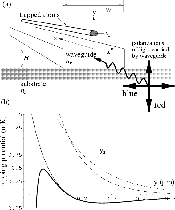
In this chapter we discuss a two-color trap based on the
EW fields above a single-mode, submicron optical `channel' waveguide.
The trap provides
tight confinement in two dimensions
and allows free de Broglie wave propagation in the third, forming an
atomic waveguide that could transport atoms
a between ![]() and
and ![]() above the optical guide surface.
Our proposal is to utilize the
differing vertical
evanescent decay lengths of the two polarizations carried in the
single-mode optical guide (see Figure 8.1).
The physical origin of this decay length difference is
the fact that the TM mode is closer to optical cut-off than the TE mode at
the same frequency.
above the optical guide surface.
Our proposal is to utilize the
differing vertical
evanescent decay lengths of the two polarizations carried in the
single-mode optical guide (see Figure 8.1).
The physical origin of this decay length difference is
the fact that the TM mode is closer to optical cut-off than the TE mode at
the same frequency.
Our proposal is reminiscent of some existing resonant enhancement schemes for EW mirrors (demonstrated with surface plasmons [71] and dielectric waveguides [109,124]) but with a radical change from a planar geometry to a linear, the mechanism for exciting the guide, and the simultaneous guiding of a second frequency of opposite detuning. It also shares the feature of two guided colors with an atom trap proposal using microsphere whispering-gallery modes[141].
Our design has many desirable
experimental features:
1) very little optical power is required to obtain large
trapping intensities since the optical bound mode has very small cross
sectional area (
![]() ),
2) the optical field is non-divergent, so can
be maintained over distances
orders of magnitude further than diffraction-limited propagation
in free space
allows,
3) the trapping potential is well-known, mechanically stable,
and insensitive
to experimental parameters other than the optical powers,
since it is defined by single-mode intensity
distributions fixed relative to a substrate,
4)
fabrication of
arrays of closely spaced atom waveguides is possible[176],
for
parallel lithography or measurement, creating ``on-chip'' integrated
atom-optical
elements,
5) the atoms are exposed providing additional optical and physical access
(a feature not shared with hollow-fiber designs), and
6)
the velocity of the atoms along
the direction of the waveguide could be controlled by standing waves in
the light carried by the
optical guide [114].
),
2) the optical field is non-divergent, so can
be maintained over distances
orders of magnitude further than diffraction-limited propagation
in free space
allows,
3) the trapping potential is well-known, mechanically stable,
and insensitive
to experimental parameters other than the optical powers,
since it is defined by single-mode intensity
distributions fixed relative to a substrate,
4)
fabrication of
arrays of closely spaced atom waveguides is possible[176],
for
parallel lithography or measurement, creating ``on-chip'' integrated
atom-optical
elements,
5) the atoms are exposed providing additional optical and physical access
(a feature not shared with hollow-fiber designs), and
6)
the velocity of the atoms along
the direction of the waveguide could be controlled by standing waves in
the light carried by the
optical guide [114].
Compared to a Zeeman-effect magnetic trap for neutral atoms, far-detuned optical dipole-force traps can have comparable trapping times, but typically an order of magnitude less depth and transverse mode spacings than recent magnetic traps [197,97,104,59,190] (for an introduction see [22]). However, in microfabricated applications the stray magnetic fields decay as a power law with distance, whereas evanescent light fields decay exponentially (ignoring for now any scattering into free space caused by optical defects). We believe this could give guided optical traps a distinct advantage in terms of achievable density of independent atom-optical elements on a single substrate.
Also, optical traps have
the advantage that
there is no significant loss mechanism which can remove atoms
from the trap
(assuming the thermal energy is much less than the trap depth):
spontaneous events cause a small heating rate, and
non-adiabatic changes in ![]() can change the optical potential but
not the fact that the atom remains trapped.
This is to be contrasted with a non-adiabatic spin-flip
event in a magnetic trap, which
results in loss of the atom.
This makes optical waveguides particularly attractive for
incoherent transport, when the loss of coherence due to the
spontaneous events is unimportant.
Finally, optical manipulation has the advantage over magnetic manipulation
in terms of high possible switching speeds.
can change the optical potential but
not the fact that the atom remains trapped.
This is to be contrasted with a non-adiabatic spin-flip
event in a magnetic trap, which
results in loss of the atom.
This makes optical waveguides particularly attractive for
incoherent transport, when the loss of coherence due to the
spontaneous events is unimportant.
Finally, optical manipulation has the advantage over magnetic manipulation
in terms of high possible switching speeds.
This chapter is organized as follows.
In Section 8.2
we describe the dipole potential,
the exponential approximation for the EW fields, and the mechanism
for the difference in decay length.
We show how we optimized the optical guide dimensions,
in the case of a rectangular
guide on a substrate of unity refractive index (for ![]() ),
and discuss some design objectives and implementation issues.
In Section 8.3
we give simulated results for cesium atoms:
trap depth, coherence time, transverse mode spacing and Q factor, and
spontaneous heating
rate.
We also show how depth and coherence time are generally limited by only
two parameters
(the detuning and the normalized decay length difference).
We study both
the case of a substrate refractive index of unity, and in Section
8.3.3
the more realistic index of 1.32.
We describe the numerical electromagnetic finite element technique in
Section 8.4, including the accuracy achieved.
Section 8.5 is an investigation of two
potential causes of loss or
decoherence of atoms, namely interactions with the dielectric surface and
bending of the waveguide.
Finally in Section 8.6 we conclude and give some future
prospects for this proposal.
),
and discuss some design objectives and implementation issues.
In Section 8.3
we give simulated results for cesium atoms:
trap depth, coherence time, transverse mode spacing and Q factor, and
spontaneous heating
rate.
We also show how depth and coherence time are generally limited by only
two parameters
(the detuning and the normalized decay length difference).
We study both
the case of a substrate refractive index of unity, and in Section
8.3.3
the more realistic index of 1.32.
We describe the numerical electromagnetic finite element technique in
Section 8.4, including the accuracy achieved.
Section 8.5 is an investigation of two
potential causes of loss or
decoherence of atoms, namely interactions with the dielectric surface and
bending of the waveguide.
Finally in Section 8.6 we conclude and give some future
prospects for this proposal.
 |